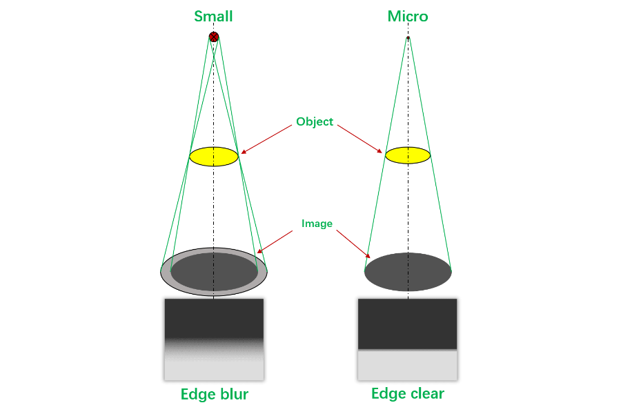
First of all, let’s understand the focal spot size. This parameter comes from the X-ray source. It affects the definition of the final imaging together with the flat panel detector. It is also an important parameter for the PCB X-ray inspection system.
X-rays are generated inside the X-ray source. The filament that acts as the cathode emits an electron beam and bombards the anode target. 99% of the kinetic energy is converted into thermal energy, and 1% of the kinetic energy is emitted in the form of photons. Then, the area where the electron beam strikes the anode target is the focus spot of the X-ray source.
Therefore, the focal spot can be considered as the place where X-rays are generated, just like the shadows produced by light. The larger the area of the light source, the more blurred the image projected on the flat panel detector. As shown below:

Focal spot size


